Quantum electron transport in ohmic edge contacts between two-dimensional materials
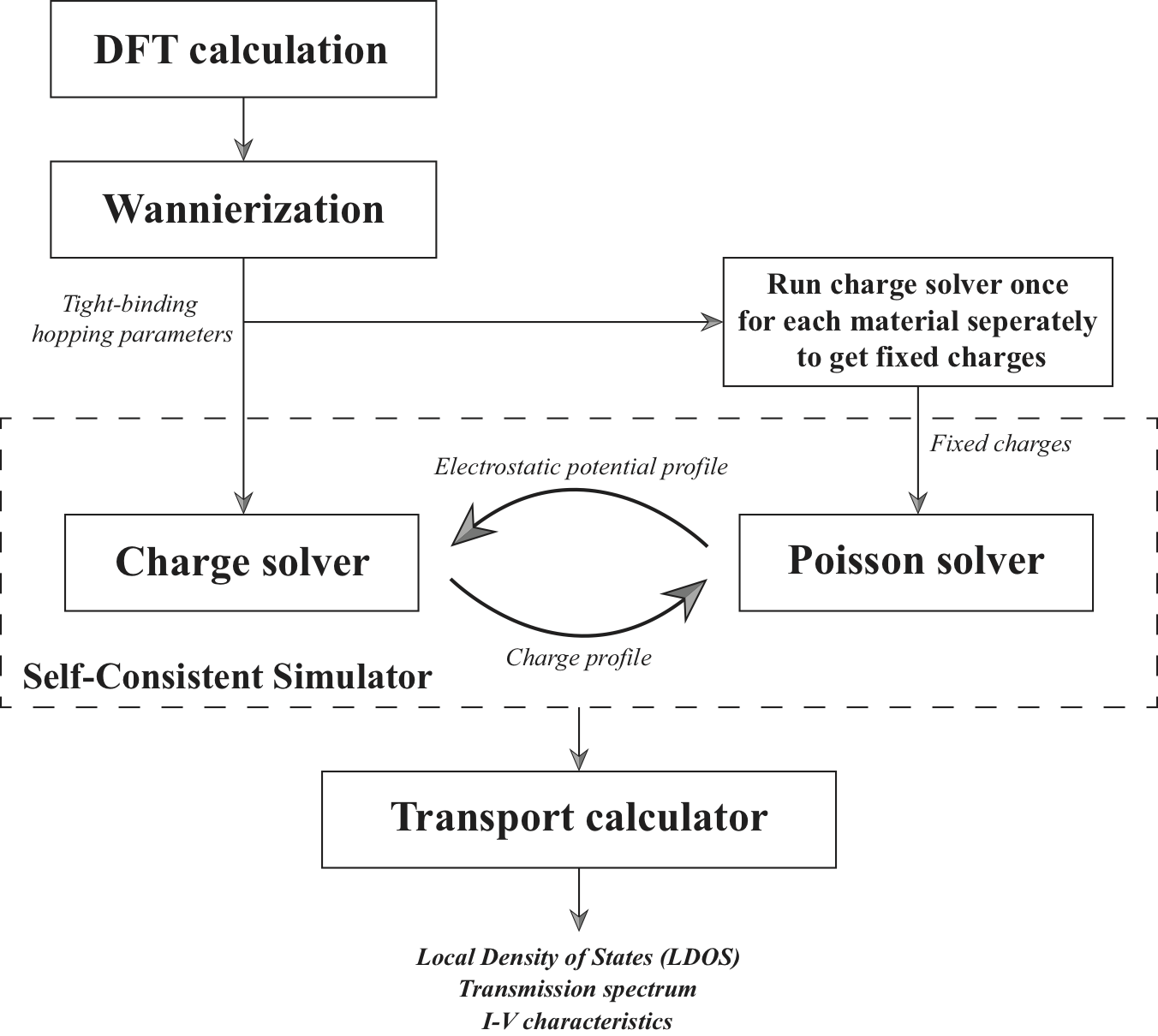
The metal-semiconductor contact is a major factor limiting the shrinking of transistor dimension to further increase device performance. In-plane edge contacts have the potential to achieve lower contact resistance due to stronger orbital hybridization compared to conventional top contacts. However, a quantitative understanding of the electron transport properties in the edge contact is still lacking. In this work, we present full-band atomistic quantum transport simulations of the graphene/MoS$_2$ edge contact. By using a Wannier function basis to accurately describe the electronic bands, together with a full self-consistent solution of the electrostatics, we are able to efficiently model device structures on a micron scale, but with atomic level accuracy. We find that the potential barrier created by trapped charges decays fast with distance away from the interface, and is thus thin enough to enable efficient injection of electrons. This results in Ohmic behavior in its I-V characteristics, which agrees with experiments. Our results demonstrate the role played by trapped charges in the formation of a Schottky barrier, and how one can reduce the Schottky barrier height (SBH) by adjusting the relevant parameters of the edge contact system. Our framework can be extended conveniently to incorporate more general nanostructure geometries. For example, a full 3D solution of the electrostatics will also lead to better modeling of the electrical potential. Furthermore, better ab-initio calculations can be conveniently added to our methods to further improve their accuracy.
PDF Abstract