Embedding physics domain knowledge into a Bayesian network enables layer-by-layer process innovation for photovoltaics
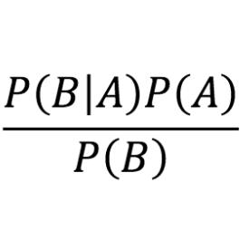
Process optimization of photovoltaic devices is a time-intensive, trial-and-error endeavor, which lacks full transparency of the underlying physics and relies on user-imposed constraints that may or may not lead to a global optimum. Herein, we demonstrate that embedding physics domain knowledge into a Bayesian network enables an optimization approach for gallium arsenide (GaAs) solar cells that identifies the root cause(s) of underperformance with layer-by-layer resolution and reveals alternative optimal process windows beyond traditional black-box optimization. Our Bayesian network approach links a key GaAs process variable (growth temperature) to material descriptors (bulk and interface properties, e.g., bulk lifetime, doping, and surface recombination) and device performance parameters (e.g., cell efficiency). For this purpose, we combine a Bayesian inference framework with a neural network surrogate device-physics model that is 100× faster than numerical solvers. With the trained surrogate model and only a small number of experimental samples, our approach reduces significantly the time-consuming intervention and characterization required by the experimentalist. As a demonstration of our method, in only five metal organic chemical vapor depositions, we identify a superior growth temperature profile for the window, bulk, and back surface field layer of a GaAs solar cell, without any secondary measurements, and demonstrate a 6.5% relative AM1.5G efficiency improvement above traditional grid search methods.
PDF Abstract

